 Co., Ltd.")


One article to take you to understand the history of the development of scanning probe microscope
Release time:
2024-08-20
The history of Scanning probe Microscope (SPM) is a remarkable scientific progress, which lays the foundation of nanoscience and nanotechnology. Since the 1980 s, the emergence and preservation of SPM has not only enabled scientists to observe and manipulate materials with atomic and molecular precision, but also promoted research in many related fields. The following are the key milestones in SPM development:
The history of Scanning probe Microscope (SPM) is a remarkable scientific progress, which lays the foundation of nanoscience and nanotechnology. Since the 1980 s, the emergence and preservation of SPM has not only enabled scientists to observe and manipulate materials with atomic and molecular precision, but also promoted research in many related fields. The following are the key milestones in SPM development:
Early 1980 s-Invention of the Scanning Tunneling Microscope (STM)
1981: German physicists Gerd Binnig and Heinrich Rohrer invent the scanning tunneling microscope (STM) at the IBM Zurich Research Laboratory. The invention of STM marked the beginning of scanning probe microscopy.[1]

Binning.

Lorrell
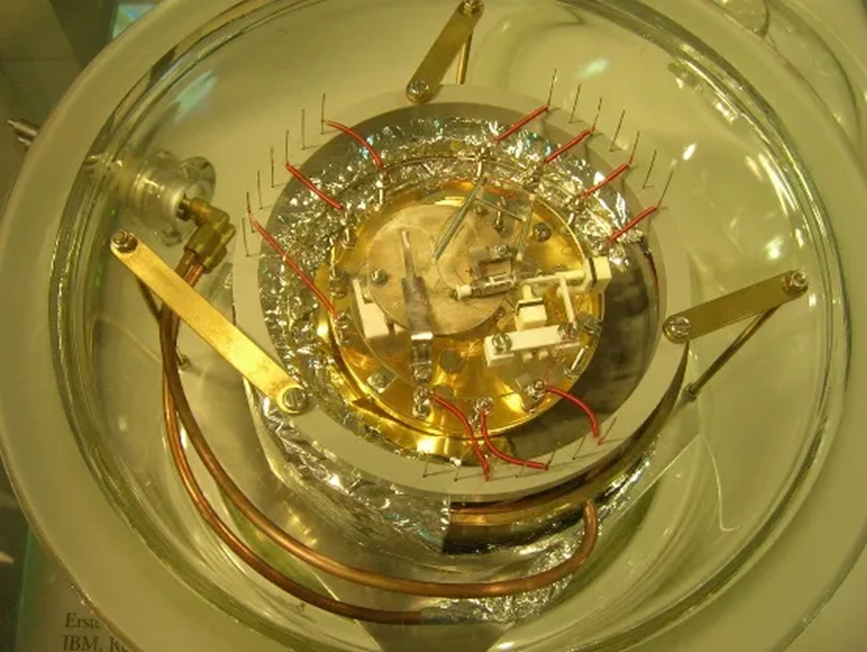
The world's first scanning tunneling microscope[2]
1986: Binning and Lorrell receive the Nobel Prize in Physics for their invention of the STM. Their work demonstrated that STMs can be imaged at atomic-level resolution, opening up a new understanding of the structure of matter.
1989: IBM scientists demonstrate a technique capable of manipulating individual atoms. Using a scanning tunneling microscope, they arranged 35 individual xenon atoms on a cold crystal substrate of nickel, spelling out the three letters of the company's acronym. This is the first time that atoms have been precisely positioned on a plane.[3]
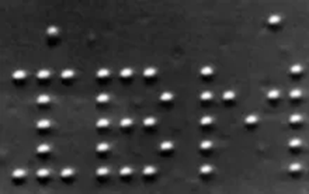
Spell "IBM" with 35 xenon atoms"
mid-1980s-Development of atomic force microscopy (AFM)
1986: Binning, Calvin Quate and Christoph Gerber invent the atomic force microscope (AFM). AFM can work on non-conductive materials, expanding the application range of SPM technology. [4]AFM uses the van der Waals force between the probe and the sample surface for imaging, and can be operated in vacuum, air and liquid environments, so it has a wide range of applications in materials science and biological research.
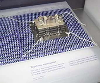
The first atomic force microscope
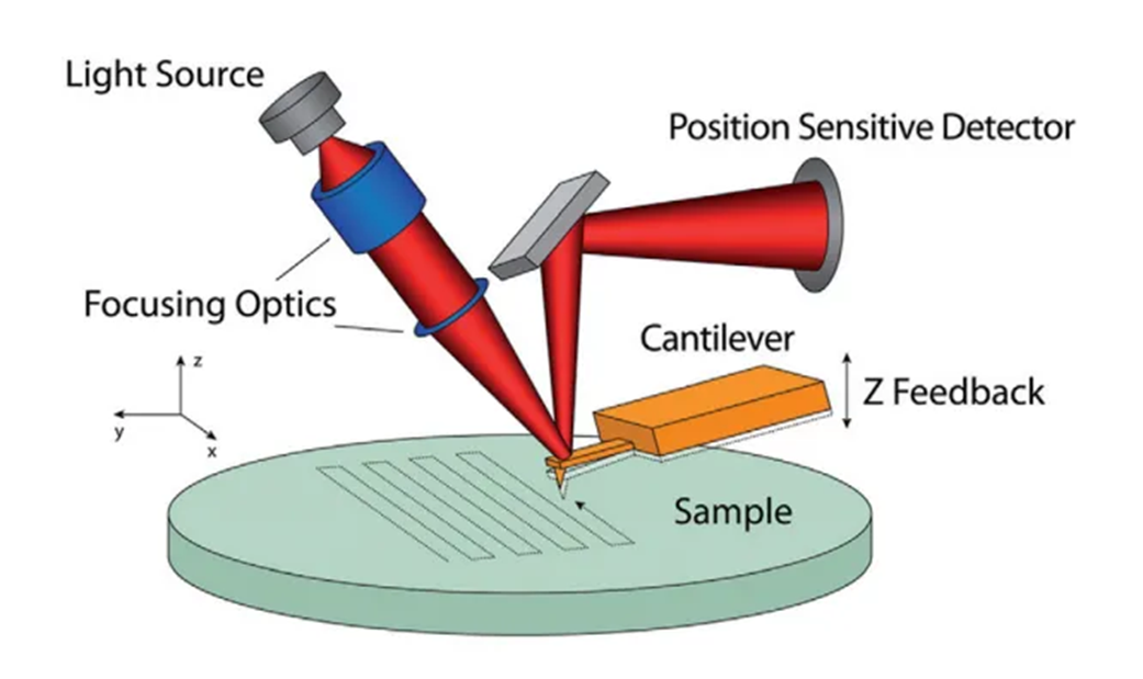
Schematic diagram of atomic force microscope
1990 s-Expansion and diversification of scanning probe microscopy
1. Magnetic force microscope (MFM): Magnetic force microscope (MFM) was invented in the late 1980 s and early 1990 s. By using a probe with a magnetic coating, the measurement probe interacts with the surface of the sample to achieve Nanoscale high-resolution magnetic domain imaging. This innovation allows researchers to gain insight into the magnetic properties of the material.
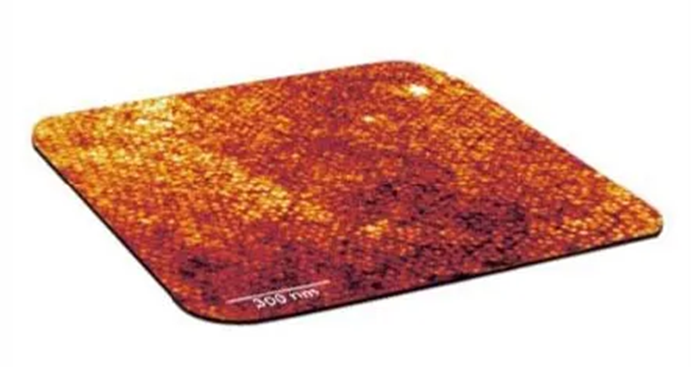
Study on Microstructure Defects by Low Temperature High Magnetic Field Magnetic Force Microscopy
2. Electrostatic force microscope (EFM): Electrostatic force microscope (EFM) was invented by Stephen Culps (Stephen Kalb) and Horst F. Falmer (Horst F.Hamann) in the late 1980 s and early 1990 s. It measures electrostatic force changes through charged probes and realizes nanoscale high-resolution electrical imaging. EFM is widely used in the study of semiconductor materials, charge storage devices and nanoelectronics.
Near-field scanning optical microscopy (NSOM or SNOM): The near-field optical microscope (NSOM) was invented by Eric Betzig and John Trautman in the late 1980 s and early 1990 s. NSOM uses a fiber optic probe with a sub-wavelength aperture to capture high-resolution optical images by confining light in a very small area and scanning the sample surface. It is widely used in materials science, biology, chemistry, and semiconductor research.
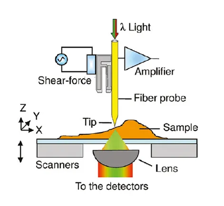
General Principles of NSOM
2000 s to the present-Further development and application of SPM technology
1. High resolution and high sensitivity:With the development of probe technology, control system and data processing technology, the resolution and sensitivity of SPM are continuously improved.
2. Multi-functional probe:Probes with specific chemical, mechanical, magnetic or mechanical properties are developed, allowing for more diverse characterization and manipulation of SPMs.
3. Multi-mode imaging:Combined with multiple imaging modalities, multiple property information of the sample can be obtained simultaneously.
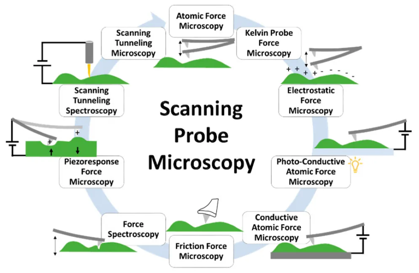
Combined multiple modes of scanning probe microscopy
4. Wafer level imaging:With the dramatic increase in the scale of integrated circuits, large samples need to be imaged.
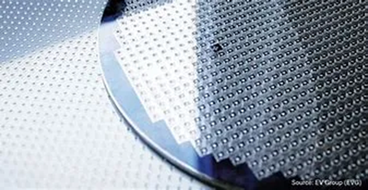
Chip Machined on Wafer
5. Application in biology: SPM is more and more widely used in the study of biological molecules and cells, which can directly observe the structure and dynamic process of biological macromolecules.
Future Outlook
The technology of scanning probe microscopy is still evolving and new techniques and applications are emerging. Multifunctional atomic force microscopes and wafer-scale atomic force microscopes developed by Zhiguo Precision Instruments support the characterization of large-size samples, andIntegrated magnetic, piezoelectric, scanning Kelvin and liquid phase analysis functions, hasExtremely low noise level, and hasAnalysis of Intelligent Data Processing Based on Deep Learning. The future will continue to focus on higher resolution, faster imaging speed and stronger multi-functional SPM equipment research to meet the needs of scientific research and industrial applications.
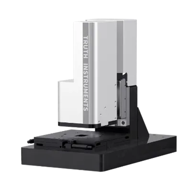
Multi-functional atomic force microscope AtomEdge independently developed by Zhizhen Company
Intelligent Analysis Algorithms for Integrated AI
Least News

Provide reliable equipment for advanced manufacturing, empowering technological innovation through precision measurement!!
Contact Information

Business Inquiries:+86-532-89267428/13335086685Manager Yao
Switchboard:+86-532-89269848
Company Address: Phase II of Changsheng Emerging Industrial Park, No. 169 Zhuzhou Road, Laoshan District, Qingdao, Shandong Province, China

WeChat Official Account

Bilibili Account