 Co., Ltd.")


Dry goods! Understanding Atomic Force Microscopy
Release time:
2024-08-20
Atomic force Microscope (AFM) is a common scanning probe microscope, which uses the interaction between the micro-arm probe and the atomic force of the sample to detect the surface structure of the material. When the probe is close to the sample, the force between the two will cause the micro-cantilever to deflect or change in amplitude. These small changes are amplified by the optical lever and then captured by the detection system and converted into electrical signals, which are transmitted to the feedback system and the imaging system (as shown in the figure below). By recording a series of changes of the probe during the scanning process, the surface topography structure information is obtained.
Atomic force Microscope (AFM) is a common scanning probe microscope, which uses the interaction between the micro-arm probe and the atomic force of the sample to detect the surface structure of the material. When the probe is close to the sample, the force between the two will cause the micro-cantilever to deflect or change in amplitude. These small changes are amplified by the optical lever and then captured by the detection system and converted into electrical signals, which are transmitted to the feedback system and the imaging system (as shown in the figure below). By recording a series of changes of the probe during the scanning process, the surface topography structure information is obtained.
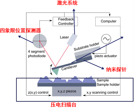
AFM system structure diagram
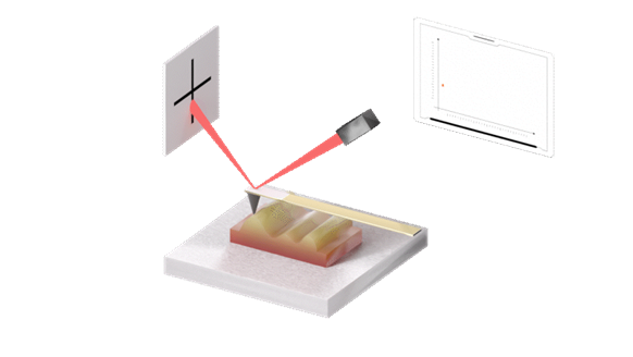
Scanning Schematic Diagram (Dynamic Diagram)
Interaction force and relative position relationship between probe tip and sample
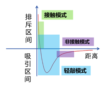
AFM imaging modes can be divided into the following three types according to the interval of the force-displacement relationship curve between the probe and the sample used during use:
(1) Contact mode: The tip of the AFM probe is in contact with the sample surface, and the distance between the two is maintained at a constant value, so that the interaction force between the tip and the sample surface atoms remains stable. This force can be maintained by controlling the microprobe to maintain a certain degree of bending. In this process, the change of the bending degree of the probe caused by the surface fluctuation of the sample can be compensated by the piezoelectric stage to return to the original state, and the compensated displacement is the morphological information of the sample surface.
(2) Tapping mode: The tip of the probe vibrates above the sample surface at a resonant frequency. The tip of the probe "taps" onto the sample surface. When the distance between the probe and the sample changes, the force applied to the probe will change, so that the amplitude of the probe vibration will also change. Determine the morphology of the sample based on the amplitude change
(3) Non-contact mode: the tip of the probe is suspended above the surface of the sample without direct contact. Although the probe does not directly contact the sample, there is still an attractive force between the tip and the sample. By detecting the change of the interaction force, the information of the surface morphology of the sample can be obtained.
Advantages of AFM:
(1) High resolution: AFM has atomic-level resolution, which can observe the tiny details of the sample surface. AFM provides a true three-dimensional surface map, not limited to two-dimensional images.
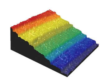
Imaging HOPG (Class B) Monoatomic Layer Steps Based on Tap Mode
(2) Non-destructive testing: AFM does not require special treatment of samples. This avoids irreversible damage to the sample, and the use of non-contact and tapping modes during the detection process causes almost no damage to the sample surface.
1.5nm silicon carbide step imaging based on non-contact mode
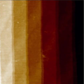
(3) Wide applicability: AFM is not only suitable for conductor samples, but also for non-conductor samples. It can be used to study various materials, including insulators, biomaterials and nano-functional materials.
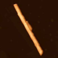
Imaging of alumina whiskers based on tapping mode
Generally speaking, AFM is a powerful surface analysis tool, which plays an indispensable role in nanotechnology, materials science, biomedicine and other fields. AFM's high-resolution imaging capabilities, applicability to a variety of samples, and flexibility to operate in different environments make it an important window for studying the nano-world. Whether in solids or liquids, AFM provides critical surface and atomic level information that drives a new chapter in scientific research and technology.
Least News

Provide reliable equipment for China's IC manufacturing, empowering technological innovation through precision measurement!
Contact Information

Business Inquiries:+86-532-89267428/13335086685Manager Yao
Switchboard:+86-532-89269848
Company Address: 393 Songling Road, Laoshan District, Qingdao, Shandong Province, China

WeChat Official Account

Bilibili Account