 Co., Ltd.")


Scanning probe microscope-multi-mode measurement
Release time:
2024-08-20
Magnetic force microscopy (Magnetic Force Microscope,MFM) is a scanning probe microscope specifically designed to image the magnetic distribution of the sample surface, obtaining information through the magnetic interaction between the probe and the sample.
An article on the (I) of expanding the mode of scanning probe microscope.
1 MFM(Magnetic Force Microscope,磁力显微镜)
Magnetic force microscopy (Magnetic Force Microscope,MFM) is a scanning probe microscope specifically designed to image the magnetic distribution of the sample surface, obtaining information through the magnetic interaction between the probe and the sample.
MFM Applications
MFM is mainly used to study the magnetic characteristics of materials, widely used in physics, materials science, electronics and other fields. Common applications include:
● Magnetic recording media: study the magnetic structure and defects of magnetic recording devices such as hard disks and magnetic tapes;
● Magnetic materials: analyze the magnetic domain structure of magnetic thin films, nanoparticles, magnetic multilayer films and other materials;
Biomagnetism: The study of naturally occurring magnetic substances in biological tissues, such as magnetic bacteria.
Application example
In the study of spin storage, taking the study of Skinman as an example, the traditional magnetic storage unit is limited by the material properties, which significantly affects the high density requirements of spin storage. Sgminzi is a kind of quasi-particle with topological properties, and its minimum size is only 3nm, which is much smaller than the magnetic tunnel junction. It is an ideal information carrier and is expected to break through the bottleneck of information storage density. The figure below is an image of the Sgoming sub-image acquired by MFM characterization.[1]
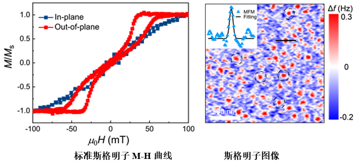
standard Sgoming sub-M-H curve Sgoming sub-image
In magnetic disk research, high-resolution magnetic images of the disk surface can be obtained by MFM, and the magnetic domain structure and distribution can be understood in detail. MFM has high spatial resolution and sensitivity, which provides important data support for the research and optimization of magnetic disk materials. The following figure shows the magnetic domain structure image of the disk surface obtained by the MFM test.
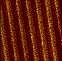
Computer floppy disk magnetic domain image
2 PFM(Piezoresponse Force Microscope,压电力显微镜)
Piezoelectric force microscopy (Piezoresponse Force Microscopy,PFM) is a scanning probe microscope used to study the piezoelectric properties of materials, using the inverse piezoelectric effect between the probe and the sample surface to image and measure the piezoelectric response of materials.
Schematic of piezoelectric response force microscopy measurements. Piezoelectric response force microscopy (PFM) works by applying a voltage V to the surface of a material with a conductive tip. In piezoelectric materials, the tip voltage V will cause a local deformation h, which is considered to be entirely due to the piezoelectric coupling. Therefore, the effective piezoelectric coefficient is taken as d33eff = h Vdocumentclass[12pt]{minimal}usepackage{amsmath}usepackage{wasysym}usepackage{amsfonts}usepackage{amssymb}usepackage{amsbsy}usepackage{mathrsfs}usepackage{upgreek}setlength{oddsidemargin}{-69pt}begin{document $}$ d_{33 }^{ mathrm{eff }}}= h/V ${document}. However, the tip voltage creates an uneven electric field under the PFM tip, which decays as we move away from the tip. The gradient of this electric field (∇ E) must induce strain in all dielectrics (including non-piezoelectric materials) through the inverse flexoelectric effect, see equation (1), which leads to the measured deformation h, which leads to the apparent piezoelectric coefficient
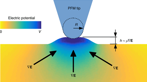
Schematic diagram of material deformation due to inverse piezoelectric effect[2]
PFM Applications
PFM is widely used in materials science and electronics, especially in the research and development of new piezoelectric materials and devices. Specific applications include:
● Ferroelectric materials: study the domain structure, switching behavior and depolarization of ferroelectric materials.
Piezoelectric devices: Analyze the performance of piezoelectric sensors, actuators, and memory devices.
Biomaterials: The study of piezoelectric effects in biological tissues, such as bones and teeth.
Application example
PbTiO3 has a significant piezoelectric effect, that is, an electric charge is generated under the action of an applied mechanical stress. This gives it important applications in ultrasonic generators, piezoelectric sensors and actuators. In the study of PbTiO3 samples, PFM can be used to obtain high-resolution piezoelectric response images of PbTiO3 surface, and to understand its domain structure and distribution in detail, which provides important data support for the research and optimization of PbTiO3 materials. The following figure shows the Piezoelectric force image of the PbTiO3 sample surface obtained by the PFM test.

3 EFM(Electrical Force Microscope, Electrostatic Force Microscope)
Electrostatic force microscopy is a type of scanning probe microscope used to measure the electro-static properties of the surface of an imaged sample. EFM obtains surface charge distribution and potential information through electrostatic force interaction between the probe and the sample surface.
Electrostatic force microscope (lift mode)[3]
EFM Applications
EFM is widely used in materials science, electronics and nanotechnology. Common applications include:
• Charge distribution: The charge distribution on the surface of the material is measured and imaged.
Surface potential: Study of the potential distribution and electrical properties of the surface of the material.
Semiconductor devices: analyze the electrical characteristics and defects in semiconductor devices.
Nanoelectronics: The study of the electrical properties of nanoscale electronic devices.
Application example
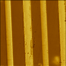
Au-Ti strip electrode electrostatic force
4 KPFM(Kelvin Probe Force Microscopy)
KPFM is a scanning probe microscope that obtains the work function and table potential distribution of the sample through the contact potential difference between the probe and the sample. KPFM is widely used in the study of surface potential changes of metals, semiconductors, biological materials and the electronic properties of nanostructures.
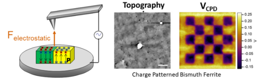
Obtaining Surface Potential of Bi-Fe Thin Film Samples by KPFM[4]
KPFM Applications
KPFM has a wide range of applications in materials science, electronics and nanotechnology. Common applications include:
Surface potential distribution: The local potential distribution on the surface of the material is measured and imaged.
● Work function measurement: Study the work function changes of materials, especially for interfaces and defects of different materials.
Semiconductor device: The potential distribution and electrical characteristics in the semiconductor device are analyzed.
Organic electronics: the study of the surface potential of organic semiconductors and organic electronic devices.
Application example

Surface potential of Au-Ti strip electrode sheet
5 SCM(Scanning Capacitance Microscope, scanning capacitance microscope)
Scanning capacitance microscopy (canning Capacitance Microscope,SCM) is a type of scanning probe microscope used to measure and image changes in capacitance at the surface of a sample. SCM can provide high-resolution images of local electrical properties through changes in capacitance between the probe and the sample surface. This microscope is suitable for studying the electrical properties of semiconductor materials and devices, such as doping concentration distribution, charge distribution and interface characteristics. SCM plays an important role in semiconductor process and material research, failure analysis, and device optimization. Through SCM, researchers can obtain nano-scale electrical properties information, thereby promoting the development and innovation of semiconductor technology.
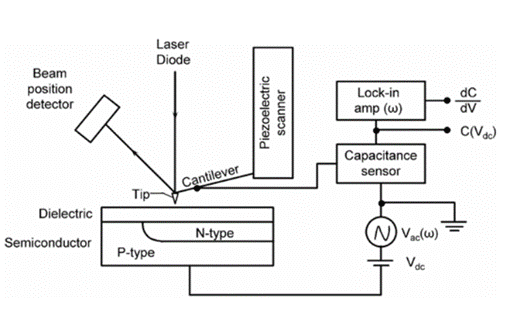
Schematic diagram of SCM principle[5]
SCM Applications
SCM is mainly used in the research of semiconductor materials and devices, and is widely used in the fields of electronics and materials science. Specific applications include:
• Doping profile: The doping concentration profile in a semiconductor material is measured and imaged.
Charge distribution: Study of charge distribution and electric fields in semiconductor devices.
● Material characteristics: analyze the capacitance characteristics and dielectric constant of different materials.
7 Brief introduction of equipment
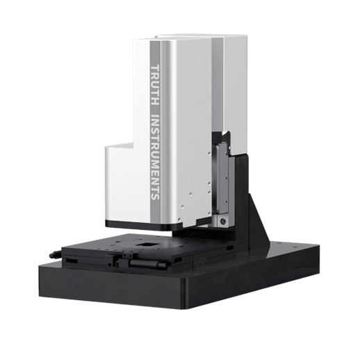
multifunctional atomic force microscope
The multifunctional atomic force microscope AtomEdge independently developed by Zhizhen Company has sub-nanometer resolution, Z-direction open-loop noise as low as 30 pm, is compatible with various physical property measurements such as magnetic domain and piezoelectric response, can work in atmospheric, liquid or vacuum environment, and has excellent stability and good scalability. As a fast and high-precision material morphology characterization tool, AtomEdge provides strong support for high-end scientific research and enterprise research and development.
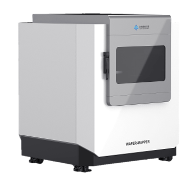
Wafer-level atomic force microscopy
The wafer-level atomic force microscope independently developed by Zhizhen Company uses a micro-cantilever probe structure to characterize the three-dimensional appearance of solid materials such as conductors, semiconductors, and insulators. The sample table is compatible with 12-inch wafers. The electric sample positioning table is combined with optical images to achieve 1μm positioning accuracy in the 300X300mm area. Laser alignment, probe approximation and scanning parameter adjustment are fully automated. It can be used in production lines for precision testing of wafer roughness.
References
[1]Li S,Du A,Wang Y,et al.Experimental demonstration of skyrmionic magnetic tunnel junction at room temperature[J].Science Bulletin,2022,67(7):691-699.
[2]Kalinin SV,Gruverman A,eds.Scanning Probe Microscopy:Electrical and Electromechanical Phenomena at the Nanoscale.Springer;2007.
[3]https://www.afmworkshop.com/products/modes/electric-force-microscopy
[4]https://www.ornl.gov/content/electrostatic-and-kelvin-probe-force-microscopy
[5]Abdollahi A,Domingo N,Arias I,et al.Converse flexoelectricity yields large piezoresponse force microscopy signals in non-piezoelectric materials[J].Nature communications,2019,10(1):1266.
Previous Page
Least News

Provide reliable equipment for China's IC manufacturing, empowering technological innovation through precision measurement!
Contact Information

Business Inquiries:+86-532-89267428/13335086685Manager Yao
Switchboard:+86-532-89269848
Company Address: 393 Songling Road, Laoshan District, Qingdao, Shandong Province, China

WeChat Official Account

Bilibili Account