Multifunctional Spin-Test Magneto-Optic Kerr Microscope
Classification
Keywords
- Product Description
- Technical Indicators
- Applications
-
Product Model:
KMPL-S
Equipment Description:
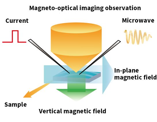
It can perform high-resolution magnetic domain imaging on magnetic materials and spintronic devices, with a resolution of up to 250 nm. It is equipped with a highly intelligent control system and a multi-functional magnetic field probe station, integrating optical imaging, multi-dimensional magnetic field, electrical transport characterization, microwave testing, and variable temperature modules into one. One-click operation can achieve the observation of magnetic dynamics processes under various excitation conditions such as magnetic field, current, spin-orbit moment, and spin-transfer moment. Equipped with a microsecond-level rapid response magnetic field, it can perform high-precision magnetic domain velocity measurement and DMI measurement.
Multi-Functional Probe Station:
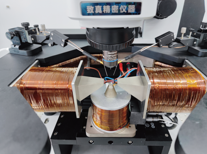
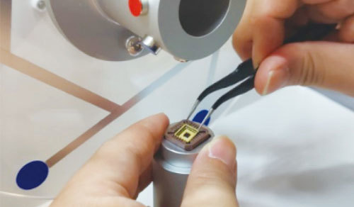
● Our multi-functional probe station provides in-plane and perpendicular magnetic fields and seamlessly integrates with multiple pairs of DC/RF probes for magneto-optical imaging and spintronic transport testing.
● With a maximum 1.4 T perpendicular magnetic field, 1 T in-plane magnetic field, and a temperature range from 4.2 K to 835 K, it is ideal for imaging research on hard magnetic materials.
Multi-Functional Control System:
1. Testing Signal Control:
● Multiple signals including perpendicular/in-plane magnetic fields, current, and microwave are synchronously applied at the microsecond (μs) level.
● Parameters such as waveform, amplitude, frequency, and relative delay of each signal are easily
adjustable.2. Image Processing
● Real-time differencing is done to eliminate background noise;
● Vibration drift is corrected automatically.
3. Signal Analysis
● Current and magnetic field testing signals are displayed in real time;
● Local (225 nm) or global hysteresis loop scans of samples are done based on Kerr imaging analysis. -
Equipment Performance
Optical Resolution 250 nm Objectives 5×, 20×, 50×, 100×, non-magnetic In-Plane Magnetic Field 1 T@air gap 5 mm; 0.5 T@air gap 10 mm; 0.3 T@air gap 16 mm Vertical Magnetic Field 0.25 T@single pole Magnetic Field Resolution PID closed-loop feedback regulation, resolution 0.05 mT Microsecond Ultrafast Pulse Vertical Magnetic Field 60 mT, rise time 0.5 μs, pulse width 1 μs - 10 μs Probe Station Compatible with 4 - 8 sets of non-magnetic probe holder Electrical Source Meter Keithley 6221, Keithley 2182A Testing Functions Magnetic domain dynamic observation, global/micro-region hysteresis loop mapping based on Kerr signals, domain wall velocity measurement, DMI measurement, anomalous Hall resistance, SOT switching, I-R hysteresis loop scanning with synchronized Kerr imaging, and curve mapping of Hall resistance changes in electronic devices under magnetic and current variations, along with corresponding Kerr images. Main Functions:
Imaging Effect:
● 225 nm (100x oil immersion objective)/450 nm (long working distance objective, compatible with
● Maximum field of view: 1.9 mm × 1.1 mm (5x objective)
It can detect magnetic variations in three atomic layers of film
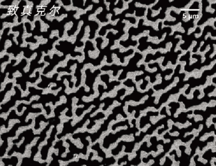
CoFeB (1.3 nm)/W (0.2)/CoFeB (0.5)
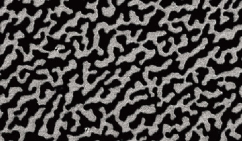
Maze domains within the film
Image Processing:
Functions, like real-time differencing, noise elimination, image drift correction, and automatic addition of scale, are all available with any image as the background.
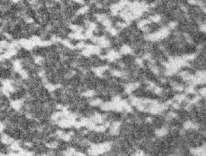
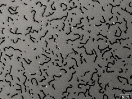
● In CoFeB (20 nm) thin film, magnetic domain reversal is achieved with [an in-plane magnetic field of 20 mT].
● Skyrmion magnetic bubbles in W/CoFeB/MgO films 
Magnetic reversal driven by SOT in CoTb ferromagnetic microwires

Domain wall motion driven by [120 mT, 5 μs] magnetic field pulses in 200 nm-wide Ta/CoFeB/MgO wires
Magnetic Field Probe Station:
● In-plane magnetic field: ≤1 T, real-time magnetic field detection resolution of 50 µT
● Three-axis orthogonal magnet switching:
Magnetic field 1: ≤1.4 T
Magnetic field 2: ≤30 mT; rise time: 100 µs
Magnetic field 3: maximum magnetic field ≥60 mT; rise time: 0.5 µs
● Up to 4 DC/RF probes can be configured, and it is compatible with 6221/2182 instruments, and suitable for electrical transport testing. It is also equipped with transport and in-situ imaging synchronization software.
Other Functions:
● Hysteresis loops can be obtained through analyzing global or local (225 nm) images.
● The hysteresis loop’s horizontal axis can be driven by in-plane, perpendicular magnetic fields, or current signals.
● A variable temperature system ranging from 4.2 K to 835 K can be configured.
● It is designed with magneto-resistance measurement and other transport testing systems and software.
● Various interfaces are reserved for user-customized modifications based on experimental requirements.
-
Applications
① Study Magnetic Material Properties
1. Detect Magnetic Material Quality
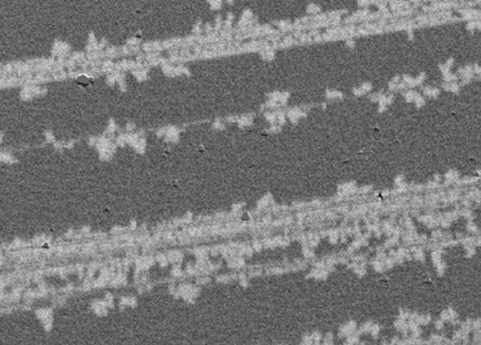
MgO(sub)/Co/Pt Sample: Defects in the film caused by the mismatch between the MgO crystal substrate and the Co lattice.
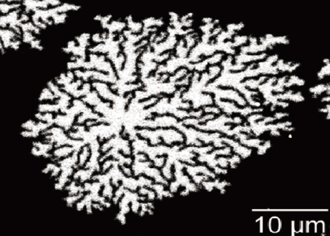
Magnetic films with poor quality exhibit snowflake-like magnetic domains during the magnetic reversal process.

High-quality magnetic films display uniform magnetic domain structures with smooth edges.
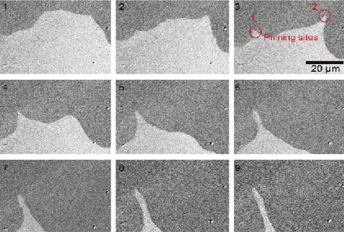
2. Detect Defect Location
At the site of a defect, deformation occurs in the motion of magnetic domain walls, resulting in a pinning effect. The defect location can be directly observed through a high-resolution objective (highlighted in red circles).
3. Hysteresis Loop Result Analysis
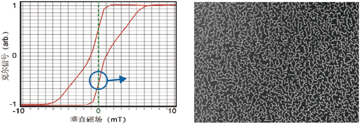
The magneto-optical Kerr microscope, with the spatial resolution advantage, can analyze the magnetic domain states corresponding to the hysteresis loop. As shown in the left image, the sample experiences spontaneous demagnetization due to the dominance of dipolar interactions over anisotropy.
② Local intrinsic magnetic parameters characterization

Simultaneous application of in-plane and perpendicular magnetic field pulses ; Combined magnetic field-driven asymmetric expansion of magnetic domains
③ Research on Magnetic Domain Wall Dynamics
1. Measurement of Magnetic Domain Wall Velocity Under the Influence of Magnetic Fields, Current, or Other Excitations
Methods:
Capture Kerr images are captured before and after applying a magnetic field/current pulse with an amplitude of B and a width of t. The difference between these images provides the domain wall motion distance, d, and then, the velocity, v = d/t is obtained.
Remarks:
To measure the ultrafast domain wall motion within a limited field of view, ultra-short signal pulses are essential. Our system features a magnetic field with a microsecond-level (μs) response time, facilitating measurements of domain wall velocities up to 200 m/s.
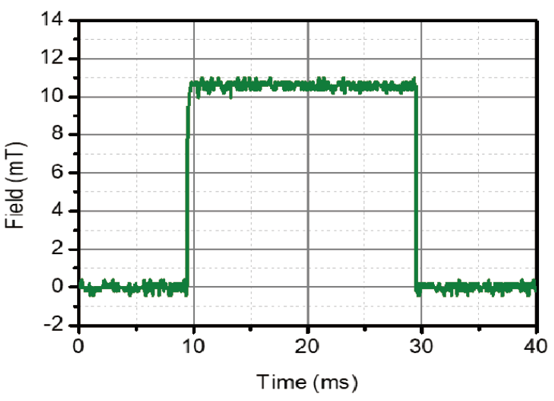
10 ms square wave magnetic field pulse
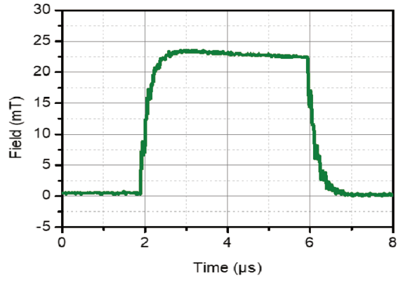
4 μs ultrafast magnetic field pulse
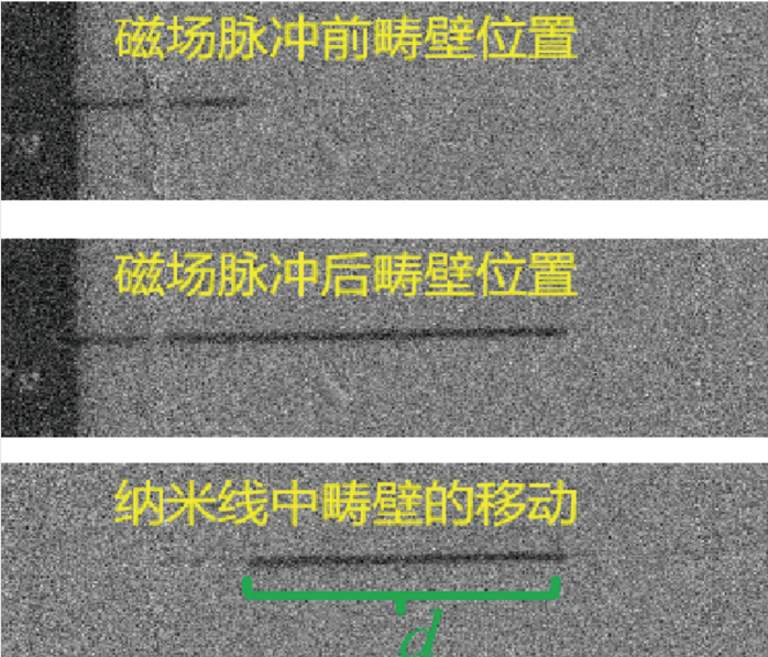
2. Observation of Magnetic Domain Wall Tension Effect
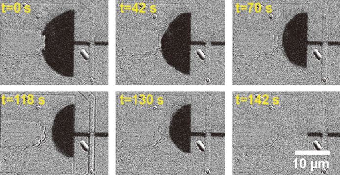
Magnetic bubbles can be produced within tiny samples by applying microsecond-level ultrafast magnetic field pulses. With the aid of this high-resolution Kerr microscope, the spontaneous contraction process of magnetic domain walls under their own tension has been observed for the first time [1-3].
3. Magnetic Domain Wall Pinning in Hall Bar
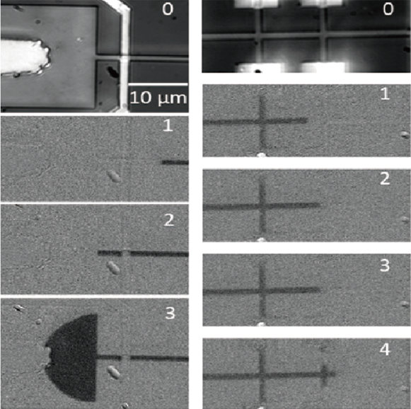
We accurately control the positioning of magnetic domain walls within nanowires using magnetic field pulses. Through this, we observe the pinning process of the magnetic domain wall and measure the depinning field [1].
[1] Xueying Zhang et al., Phys. Rev. Appl. 9,024032(2018).
[2] Xueying Zhang et al. Nanotechnology 29,365502(2018).
[3] Anni Cao et al., IEEE Magn. Lett. 9,1(2018).
④ Spintronic Transport Property Testing + Imaging
1. STT Current-Driven Magnetic Domain Wall Motion
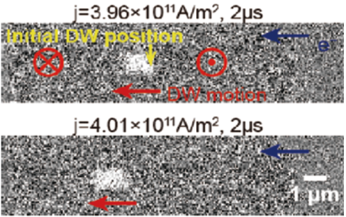
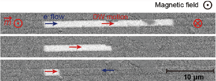
With the aid of the probes and the arbitrary waveform generators of the master control system, square waves can be applied to the sample at levels ranging from 50 nanoseconds to seconds, and then, the magnetic domain wall motion observed and velocity measured.
2. STT-Induced Magnetic Domain Wall Motion Under the Combined Action of Current and Vertical Magnetic Field
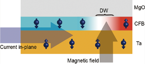
In certain materials, pure current-driven magnetic domain wall motion cannot be observed. In such cases, the equipment can synchronize microsecond-level ultrafast magnetic field pulses with the current. On this basis, the domain wall motion driven by both vertical magnetic fields and the current can be observed, and various physical effects analyzed, such as the reduction in spin polarization rates in heavy metal/ferromagnetic systems due to spin scattering effects [1].
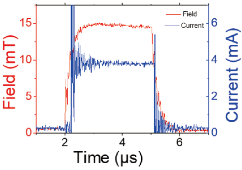
Microsecond-level synchronized magnetic field and current square wave pulses
3. Magnetic Domain Wall Motion Under the Combined Action of Current and In-Plane Magnetic Field
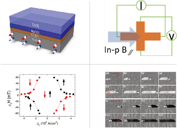
The combined action of the Hall spin current and in-plane magnetic field induces magnetic moment reversal, known as the SOT reversal. Our equipment is equipped with an in-plane magnetic field and an electrical testing system. This system can either perform electrical testing of this process, or make point-by-point analysis of the magnetic domain states corresponding to the reversal curve using synchronized camera and signal acquisition card functions [2].
4. Transport Testing Overview
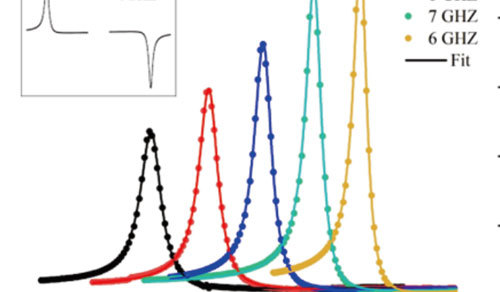
When used together with the Keithley 6221 and 2182A source meters, our system can measure the Hall effect, I-V characteristics (resistivity), and magnetoresistance (MR). Additionally, when supported by a microwave source, microwave probe, and lock-in amplifier, it can finish ST-FMR and second harmonic tests, realizing the characterization of the sample’s spin-orbit torque magnitude.
[1] Xueying Zhang et al., Phys. Rev. Appl. 11,054041(2019).
[2] Xiaoxuan Zhao et al., Nanotechnology 30,335707(2019).
Multifunctional Spin-Test Magneto-Optic Kerr Microscope
Classification
Keywords
Intention Table
Application Industry

Provide reliable equipment for advanced manufacturing, empowering technological innovation through precision measurement!!
Contact Information

Business Inquiries:+86-532-89267428/13335086685Manager Yao

Switchboard:+86-532-89269848

Company Address: 393 Songling Road, Laoshan District, Qingdao, Shandong Province, China

WeChat Official Account

Bilibili Account

