 Co., Ltd.")


Wafer-level Atomic Force Microscope
Classification
Keywords
- Product Description
- Technical Indicators
- Applications
- Customer Achievements
-
Product Model:
Atom Max
Product Overview:
The Atom Max Wafer-level Atomic Force Microscope utilizes a microcantilever probe structure to perform sub-nanometer-scale 3D scanning and imaging of solid materials such as conductors, semiconductors, and insulators, enabling topographic characterization and analysis of wafer-level large samples. Combined with optical imaging, the motorized sample stage achieves a positioning accuracy of 1 µm over a 200×200 mm area. The optical structure is integrated with the scanning head, featuring high automation and user-friendly operation.
-
Equipment Performance
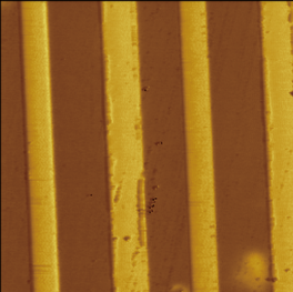
Sample size 8-inch wafer and backward compatible Scanning range 100 μm×100 μm×10 μm Scanning angle 0-360° Z-direction linearity 0.2% Noise level in the Z direction 0.06 nm Image sampling point 32×32 - 4096×4096 Working mode Contact mode, tap mode, phase imaging mode, lift mode, multi-directional scanning mode Multifunctional measurement Electrostatic force microscope (EFM), scanning Kelvin microscope (KFM), piezoelectric force microscope (PFM), magnetic force microscope (MFM);
optional: Conductive atomic force microscope (C-AFM)
-

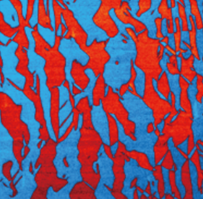
- CZTSSe film
- Scanning mode: Lift Mode(KPFM)
- Scanning range: 12 um x 12 um
- Electrostatic force of the Au-Ti strip electrode sheet
- Scanning mode: EFM (lift mode)
- Scanning range: 18μm * 18μm
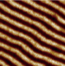
- Magnetic domains in Fe-Ni thin films
- Scanning mode: MFM (lift-mode)
- Scanning range: 14μm * 14μm
- PbTiO3-piezoelectric corresponding vertical amplitude image
- Scanning mode: PFM (contact-mode)
- Scanning range: 20μm * 20μm

- Co/Pt Thin Film
- Scanning Mode: Magnetic Force Microscopy (MFM)
- Scanning Range: 25 μm * 25 μm
Wafer-level Atomic Force Microscope
Classification
Keywords
Intention Table
Application Industry

Provide reliable equipment for advanced manufacturing, empowering technological innovation through precision measurement!!
Contact Information
Business Inquiries:+86-532-89267428/13335086685Manager Yao
Switchboard:+86-532-89269848
Company Address: Phase II of Changsheng Emerging Industrial Park, No. 169 Zhuzhou Road, Laoshan District, Qingdao, Shandong Province, China

WeChat Official Account

Bilibili Account